Everything for Electronics

Tech Forum


April 2014

555 Anomaly

I have found an interesting anomaly with the 555 IC. Everywhere I've read and looked, the #4 (reset) pin has voltage held high to allow the IC to conduct, and then dropped low to turn off (reset) the IC.

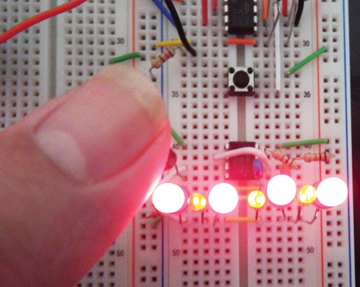
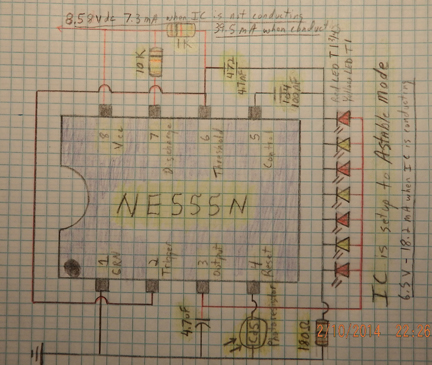
I have 8.58V at 39.5 mA at VCC (#8) pin when the IC conducts. As you can see in the, I am controlling the IC through the reset pin (#4) with a CdS photocell photoresistor. When light is removed from the CdS photocell and the IC conducts, it sends 6.5V at 18.2 mA to the output (#3) pin and LEDs. Apply light to
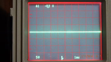
the CdS photocell and the IC stops conducting; you then get -0.2V at 0.0 mA at the output (#3) pin. Since I added a 4.7 mF electrolytic capacitor to the output pin, the IC now conducts 7V to the LEDs.

I am an electronics hobbyist who has been learning electronics for one year. I welcome any comments and ideas anyone has about what is going on with the IC.

Schematic

Scope 6.5V

Scope .2V

LEDs

**3/28/14 Update from original question.
I made a mistake on the schematic - the ceramic caps & LED's do not share the same ground line. I also removed the LED resistor and gave them each their own 470ohm resistor to lower the current.

#4141
Robert Calk Jr.
via email


Answers

Reader Robert Calk Jr. writes that he has found an interesting anomaly with the NE555 integrated circuit. (IC) Although I cannot answer his specific questions here, I can relate an experience illustrating a similar issue, that I had some years ago when the company I was with was assembling under contract a printed wiring assembly intended for use as a trailer brake controller, by a large well-known company. Thousands of assemblies were involved.


Anyway, the design was theirs, and we as assemblers were required to follow their bill of material exactly. At the heart of the controller was a 555 IC used in generating the pulse width modulated output to the brake "pucks" on the trailer.


To make a long story short, we eventually found out that the designer had unwittingly made use of and designed into his circuit, an undocumented feature or "anomaly" of the particular brand of 555 IC used. I am not sure now, but it may have been a National Semi part. In any case we eventually had supply problems and had to source the 555 from another manufacturer. Guess what, that brand did not work properly in the circuit. Neither did 555's from any other manufacturers!


The lesson here, is that a common industry parametric specification for an IC like the simple 555, or any other for that matter, will likely be closely adhered to by all suppliers of the part. However, the internal circuitry on the chip inside the IC from each supplier, may be quite different from one to another, and may well have characteristics outside of those on the data sheet.


My best advice is to look for and download application notes re the 555, that may be available from some different manufacturers.

Don Dorward
via email

The NE 555 is setup in astable (free-running) mode so it is oscillating. The output signal would be a square wave at the astable frequency. You measured the average DC output as 6.5 volts. Adding the 4.7µF capacitor is a filter to the output, and the new measured DC output is 7 volts.


To verify this, remove the 4.7µF capacitor, and use your oscilloscope to see the waveform at the output. Then reconnect the capacitor and read it again.

Raymond Ramirez
via email

In TechForum "555 Anomaly" Robert Calk, Jr described the strange action of a 555 Astable Mode circuit. First of all the circuit on your diagram is not wired as an Astable Mode 555 device or any other 555 circuit with which I am familiar. There should be a voltage divider from the +Vcc to pins 2/6 and 7 but you have drawn the 10K resistor as an "input" resistor for pin 7 (discharge) and the 1K resistor as an "input" resistor for pins 2 (Trigger) and 6 (Threshold). Pins 2, 6 and 7 have the Vcc voltage applied, NOT the voltages needed to operate the 555's comparators. Plus, the 4.7nF (0.0047 micro-F) and 100nF (0.1 micro-F) capacitors are routed to ground via the 180 ohm resistor (bad practice because any noise on pins 2, 5 and 6 will produce a noise voltage across the 180 ohm resistor which could affect the circuits operation (e.g, false triggering).


I am not sure what you are trying to do with this circuit but it looks like you are trying to turn on the LED's when the CdS photoresistor is covered. The 555 is used for timing, which is not needed in your project, so getting the same result could be easier using a digital logic circuit such as a 7404 hex inverter using the CdS cell to trigger one inverter pin (with pull up resistor to Vcc for light ON when cell uncovered or CdS cell as the pull up resistor for light ON with cell covered).


I think your circuit turns ON the LED's with the CdS cell covered because the extra resistance between pin 4 (Reset) and ground causes pin 4 to go to a "High" via internal connections, thus putting the 555 output in the set or "High" state which powers the LED's.


Get a data sheet for the 555 and see how it should be configured. A good electronics tutorial from the Internet is also advisable.

Tim Brown
Honea Path, SC

Your description of the behavior of your 555 circuit does not suggest anomalies but rather — as an old engineer once told me — "the circuit will always work the way you wire it." The 4.7 µF capacitor across the output terminal is putting an abnormal stress on the pullup circuit within the device. Voltage observed on pin 4 (/RESET ) is normal for open-circuit conditions.
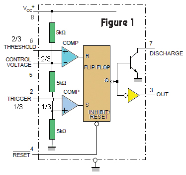
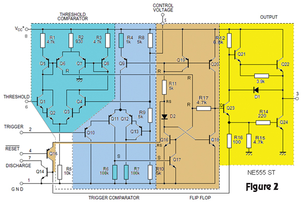
In order to use the 555 effectively, you need to know what's inside the device and how it works. When I design a 555 into a circuit, I always generate a schematic symbol that is more than just a rectangle with eight named pins. Rather, I show what's inside it — an equivalent circuit — because several years later I'll probably not remember exactly how one works and the added detail helps. Figure 1 shows the equivalent circuit of a 555 and Figure 2 shows its internal circuitry. Look at Q21 and Q22 in Figure 2 for some insight into what the 4.7 µF load might be placing on the circuit.
In the equivalent circuit, you'll see that the output is driven by a set/reset (SR) flip-flop which also has an overriding active-low master reset input (that is, you must pull the /RESET input to ground in order to reset the device). The Set (S) and Reset (R) inputs to the flip-flop are driven  by comparators which are biased to 2/3 Vcc and 1/3 Vcc, respectively. If Vcc = 12 volts, then 1/3 Vcc = 4 volts and 2/3 Vcc = 8 volts. If the THRESHOLD input is made greater than 2/3 Vcc, the flip-flop will be reset and OUT (pin 3) will fall (to ground). If the TRIGGER input is made less than 1/3 Vcc, the flip-flop will be set and the OUT erminal will rise to Vcc.

In your application, the circuitry controlling the 555 can be simplified.  Remove all of the components. Connect pins 2 (TRIGGER) and 6 (THRESHOLD) together. Connect this 2+6 pair through a pullup resistor to Vcc. Connect the 2+6 pair through your CdS photoresistor to ground. Choose the pullup resistor value such that a "dark" condition makes pins 2+6 rise to greater than 2/3 Vcc, and such that the "light" condition makes them fall to less than 1/3 Vcc. If you want the opposite behavior, reverse the circuit. Pull pins 2+6 to ground through the resistor and connect the fixed end of the CdS photoresistor to Vcc.

Finally, I caution you about paralleling LEDs. There is nothing to guarantee that they will all operate at precisely the same terminal voltage.   Proper usage dictates that each has its own current-limiting resistor, and then you wire the eight LED+resistor pairs in parallel.

There are many, many articles on the Internet regarding 555 circuits, as well as application notes from Signetics, Phillips, and Texas Instruments. I recommend them to you. Good luck.

Peter A. Goodwin
via email