The ‘555 timer’ is a popular and versatile bipolar IC that is specifically designed to generate accurate and stable C-R — defined timing periods, for use in a variety of monostable ‘one-shot’ pulse generator and astable squarewave generator applications. This article shows practical ways of using the IC in a variety of useful astable multivibrator or squarewave generator applications.
555 ASTABLE OPERATION

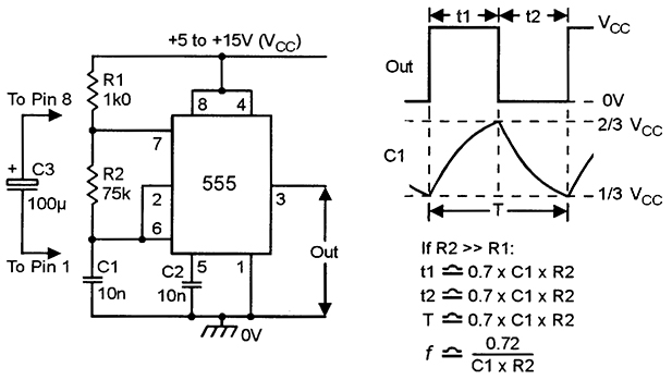
FIGURE 1. Circuit and waveforms of a basic 1 kHz 555 astable multivibrator, with optional RFI suppression via C3.
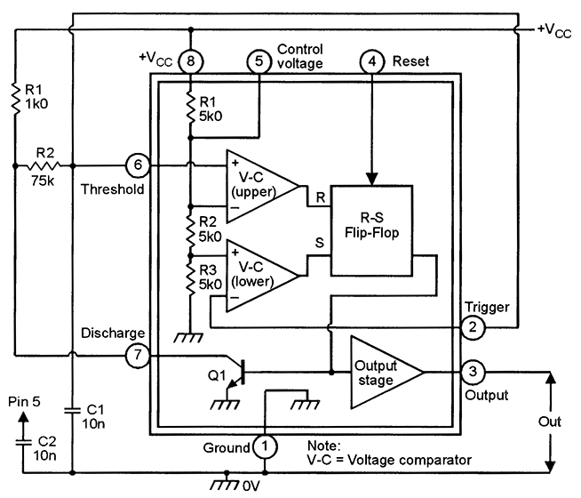
The eight-pin bipolar 555 IC can be used as a free-running astable multivibrator by wiring it in the basic configuration of Figure 1, with TRIGGER pin 2 shorted to the pin 6 THRESHOLD terminal, and timing resistor R2 wired between pin 6 and DISCHARGE pin 7. To understand the circuit operation, relate the following explanation to the 555 functional block diagram of Figure 2.

FIGURE 2. Functional block diagram (within the double lines) of the 555 timer IC, with external connections for use as a basic 1 kHz astable multivibrator.
When power is first applied to this circuit C1 starts to charge exponentially via R1-R2 until eventually the C1 voltage rises to 2/3 Vcc, at which point DISCHARGE pin 7 switches low and starts to discharge C1 exponentially via R2 until eventually the C1 voltage falls to 1/3 Vcc, and TRIGGER pin 2 is activated, thus initiating a whole new timing sequence, which repeats ad infinitum, with C1 alternately charging towards 2/3 Vcc via R1-R2 and discharging towards 1/3 Vcc via R2 only.

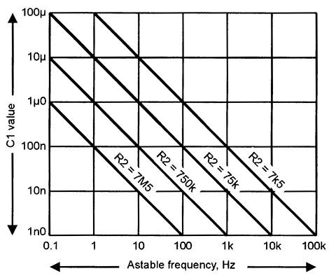
FIGURE 3. Relationship between C1, R2, and 555 astable frequency when R2 is large relative to R1.
Note that if R2 is very large relative to R1 the operating frequency is set by R2 and C1, and an almost symmetrical squarewave output is developed on pin 3 and a non-linear triangle waveform appears across C1; Figure 3 shows the consequent relationship between frequency and the C1-R2 values. In practice, the R1 and R2 values can be varied from 1k0 to many megohms; note, however, that R1 affects the circuit’s current consumption, since pin 7 is effectively grounded during half of each cycle. Also note that the waveform’s duty cycle or mark-space ratio can be varied by suitable choice of the R1 and R2 ratios.

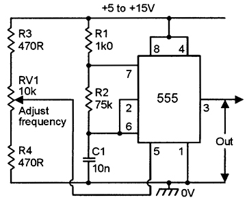
FIGURE 4. Variable-frequency (650 Hz-7.2 kHz) squarewave generator).
Figure 4 shows how the operating frequency can be made variable by replacing R2 with a series-wired fixed and a variable resistor. With the component values shown, the frequency can be varied from about 650 Hz to 7.2 kHz via RV1; the frequency span can be further increased by selecting alternative values of C1.
MARK-SPACE CONTROL
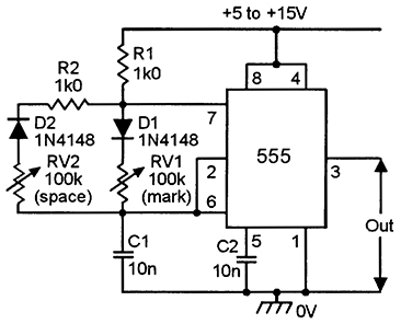
In each operating cycle of the Figure 1 circuit, C1 alternately charges via R1-R2 and discharges via only R2. Consequently, the circuit can be made to generate a non-symmetrical waveform with any desired mark/space (M/S) ratio by suitably selecting the R1 and R2 values. Figures 5 to 8 show ways of making the M/S ratios fully variable.

FIGURE 5. Astable with mark and space periods independently variable from 7 µS to 750 µS.
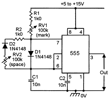
Figures 5 and 6 give independent control of the mark and space periods. In Figure 5, C1 alternately charges via R1-D1 and RV1, and discharges via RV2-D2 and R2. In Figure 6, C1 charges via R1-RV1 and D1, and discharges via RV2-D2 and R2. In both cases, the mark and space periods can each be varied over a 100:1 range; the frequency varies as the M/S ratio is altered.

FIGURE 6. Alternative version of the Figure 5 circuit.
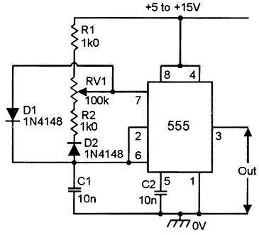
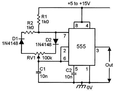
Figures 7 and 8 show ways of altering the M/S ratio without significantly altering frequency; here, the mark period increases as the space period decreases, and vice versa, so the total period of each cycle is constant. The most important waveform feature of these circuits is their ‘duty cycle’ (the relationship between the mark and total periods of each cycle), and this is variable from 1 to 99 percent via RV1.

FIGURE 7. 1.2 kHz astable multi with duty cycle variable from 1 to 99 percent.
In Figure 7, C1 alternately charges via R1-D1 and the upper half of RV1, and discharges via D2-R2 and the lower half of RV1. In Figure 8, C1 charges via R1-D1 and the right-hand half of RV1, and discharges via D2-R2 and the left-hand half of RV1. Each circuit operates at about 1.2 kHz with the C1 value shown.

FIGURE 8. Alternative version of the Figure 7 circuit.
A ‘PRECISION’ ASTABLE
Note from the description of basic astable operation that in the initial half-cycle of operation, C1 charges from zero to 2/3 Vcc, but that in all subsequent half-cycles it either discharges from 2/3 Vcc to 1/3 Vcc or charges from 1/3 Vcc to 2/3 Vcc; the initial half-cycle of astable operation thus has a longer period than all subsequent half-cycles.

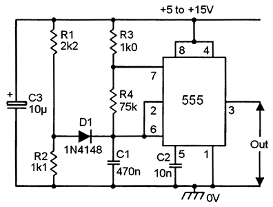
FIGURE 9. ‘Precision’ low-frequency (20 Hz) astable.
In some special applications, this large period discrepancy may cause problems; they can be overcome by adding an external voltage divider and diode to bias C1 to slightly below 1/3 Vcc (rather than to zero volts) at the moment of switch-on, as shown in Figure 9. Here, R1 rapidly charges C1 to 1/3 Vcc via D1 at initial switch-on, but all C1 charging is subsequently controlled by R3 and/or R4 only.
ASTABLE GATING
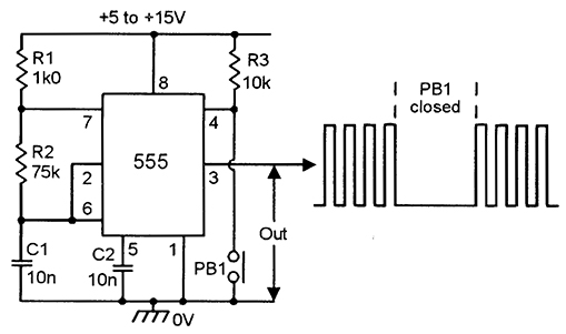
The 555 astable can be gated on and off, via either a switch or an electronic signal, in several ways. One way is via the pin 4 RESET terminal, and Figures 10 and 11 show ways of gating the astable via this pin and a push-button switch. The 555 action is such that the astable is enabled if pin 4 is biased above 0.7V, but is disabled (with its output low) if pin 4 is pulled below 0.7V by a current greater than about 0.1 mA (by grounding pin 4 via 10k or less).

FIGURE 10. Gated 1 kHz astable with ‘press-to-turn-on’ operation.
Thus, Figure 10 is normally gated off by R3, but can be turned on by closing PB1, and Figure 11 is normally on, but can be gated off by closing PB1; these circuits can also be gated electronically via pin 4.

FIGURE 11. Gated 1 kHz astable with ‘press-to-turn-off’ operation.
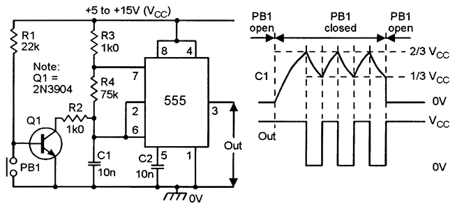
Note in Figure 10 that precise circuit waveforms are shown, and that the duration of the initial half-cycle is far longer than all others, and that C1 takes a fairly long time to decay to zero when the astable is first gated off again (the Figure 11 circuit has similar characteristics).

FIGURE 12. Alternative gated 1 kHz astable with ‘press-to-turn-on’ operation.
Figure 12 shows another way of gating the 555 astable. Q1 is normally biased on via R1 and thus acts like a closed switch that (via R2) pulls the C1-R4 junction low and stops the astable operating, but when PB1 is closed, Q1 is turned off and the astable operates in the normal way.
Note that when the astable is gated on, the initial half-cycle is again far longer than all others, etc., and that the pin 3 output terminal is high when the astable is off.

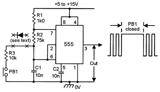
FIGURE 13. Alternative gated 1 kHz astable with ‘press-to-turn-off’ operation.
Figure 13 shows the above circuit modified to give ‘press-to-turn-off’ operation by replacing Q1 with a push-button switch. A digital signal can be used to gate this circuit by wiring a diode as shown and removing PB1, in which case, the circuit will turn off when the gate signal is below 1/3 Vcc.

FIGURE 14. ‘Precision’ version of the Figure 12 circuit.
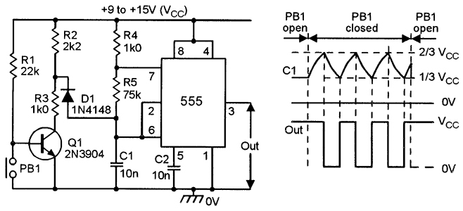
To complete this look at gating techniques, Figure 14 shows the Figure 12 circuit modified to give ‘precision’ operation.
Here, when PB1 is open Q1 is saturated, so R2-R3 pulls the R5-C1 junction to just below 1/3 Vcc via D1, thus gating the astable off, but when PB1 is closed, Q1 turns off and D1 is reverse-biased via R2, and the astable is thus free to operate.
Note that when PB1 is first closed C1 charges from an initial value of almost 1/3 Vcc, and the duration of the initial half-cycle is thus similar to all others.
FM AND PPM
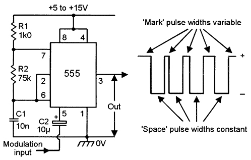
All the 555 astable circuits shown so far can be subjected to frequency modulation (FM) or to pulse-position modulation (PPM) by simply feeding the modulation signal to pin 5 (which connects to the IC’s internal divider chain); this modulation signal may be an AC signal that is coupled to pin 5 via a blocking capacitor, as shown in Figure 15, or it may be a direct-coupled DC signal, as in Figure 16.

FIGURE 15. Method of applying AC-coupled FM or PPM to the 555 astable.
The 555’s astable action is such that the pin 5 voltage influences the width of the mark, but not the space part of each cycle, and thus provides both PPM and FM actions.

FIGURE 16. Method of applying DC-coupled FM or PPM to the 555 astable.
These types of modulation are useful in special waveform generator applications, as in various electronic siren and alarm-call generator circuits.
‘555’ SIRENS AND ALARMS
One very popular application of the 555 astable circuit is as a speaker-driving siren or alarm-call generator, and Figures 17 to 22 show a selection of circuits of this type.

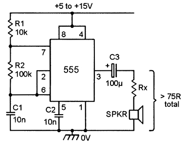
FIGURE 17. Low-power (750 mW max) 800 Hz monotone alarm-call generator.
Figure 17 shows an 800Hz monotone alarm-call generator circuit that can be used with a 5V to 15V supply and with any speaker impedance; note that Rx is wired in series with the speaker, to give a total load impedance of 75 ohms (to limit peak output currents to 200 mA).

FIGURE 18. Medium-power 800 Hz alarm-call generator.
Available alarm output power depends on the speaker impedance and supply voltage values; i.e., it is 750 mW at 75R at 15V, etc. Figure 18 shows how to boost the output power of the above circuit to several watts via Q1.
Note that the resulting high output currents may modulate the supply voltage, and D1 and C3 help isolate the 555 from this modulation; D2 and D3 clamp the inductive switching spikes of the speaker and thus protect Q1 from damage. This booster circuit is also used in the alarm circuits of Figures 19 to 22.

FIGURE 19. Pulsed-tone (800Hz) alarm-call generator.
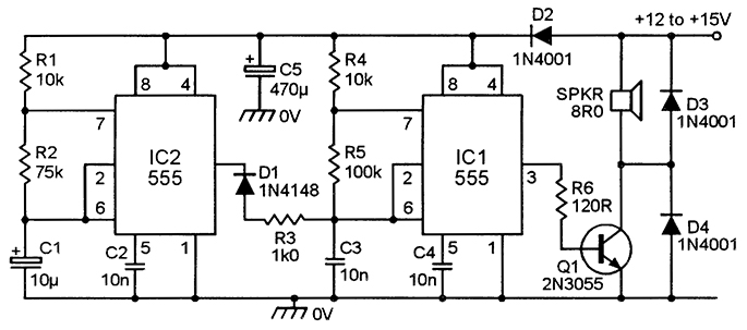
Figure 19 shows a pair of 555 astables used to make a pulsed-tone 800 Hz alarm-call generator; IC1 acts as the 800 Hz generator, and is gated on and off once per second via IC2 and D1.

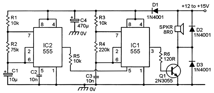
FIGURE 20. Warble-tone alarm-call generator simulates British police car siren.
Figure 20 shows a warble-tone alarm-call generator that simulates the sound of a British police car siren. IC1 is again wired as an alarm tone generator and IC2 as a 1 Hz astable but, in this case IC2 output is used to frequency modulate IC1 via R5, the action being such that IC1’s frequency alternates between 440 Hz and 550 Hz at a 1 Hz cyclic rate.

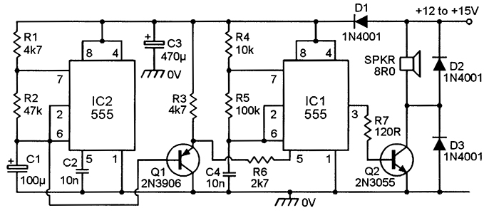
FIGURE 21. ‘Wailing’ alarm simulates American police car siren.
Figure 21 shows a ‘wailing’ alarm that simulates an American police car siren. IC2 is a low-frequency (6s) astable that generates a ‘ramp’ waveform that is buffered via Q1 and used to frequency modulate tone generator IC1 via R6.
IC1 has a mid-frequency of about 800Hz, and the modulation action is such that its output tone starts at a low frequency, rises for 3s to a peak value, then falls back again for 3s, and so on ad infinitum.

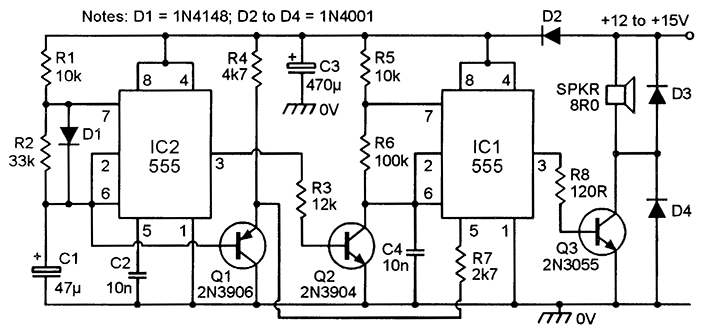
FIGURE 22. ‘Red alert’ siren simulates Star Trek alarm signal.
Finally, Figure 22 shows an alarm that simulates the ‘red alert’ sound used in Star Trek programs; this sound starts at a low frequency, rises for 1.15s to a high tone, ceases for 0.35s, and then repeats ad infinitum.
IC2 is a 1.5s non-symmetrical astable that generates a fast rising, but slowly falling sawtooth across C1; this waveform is buffered via Q1 and used (via R7) to frequency modulate IC1, making its frequency rise slowly during the falling parts of the sawtooth, but collapse rapidly during the rising part.
The rectangular pin 3 output of IC2 gates IC1 off via Q2 during the collapsing part of the signal, so only the rising parts of the alarm signal are, in fact, heard. NV

