With TJ Byers
MOSFET Basics
Question:
I don’t know that much about MOSFETs or FETs in general. Can you explain what makes them tick?
— Bob J.
Answer:
Ray Marston did a very good job of describing FETs and MOSFETs in his series "FET Principles And Circuits" in Nuts & Volts. But it focuses mostly on low power devices, which behave differently than high-power FETs. Let me try to explain.
The original transistor — invented in 1947 by a team of John Bardeen, William Shockley, and Walter Brattain at Bell Telephone Labs — was a bipolar device that amplified a small input current into a higher output current, as opposed to amplifying a small input voltage into a higher output voltage. Let me tell you, for us vacuum tube (valve) guys, it was a quantum leap in thinking about circuit design. I can’t count the number of CK722 transistors I fried by trying to apply voltage rules to a current device.
Somewhere between 1960 and 1963 the epitaxial deposition transistor evolved into the junction field-effect transistor — JFET. Like the vacuum tube, the JFET is a voltage controlled device where a negative voltage is needed to “pinch” off the flow of electrons from source (cathode) to drain (plate). Cool for us tube guys, but hardly a tube substitute.
At about the same time, the metal-oxide semiconductor field-effect transistor — MOSFET — came into being and allowed us to combine tube technology with transistor. That is, an increase in voltage prompts an increase in current flow. Most “FETs” today are of this enhanced-mode type.
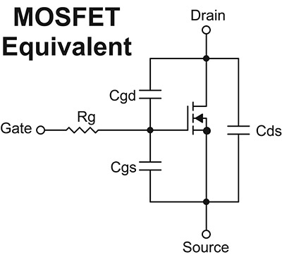
While MOSFETs can be operated in the linear region, most are used as switches — where they are either ON (conducting) or OFF (not conducting). In this mode, there are two important parameters to consider: switching time and saturation voltage. The first is the time it takes for the transistor to go from OFF to ON, and vice versa. The more time the transistor spends between the two states, the more power it dissipates. The switching times are determined by the capacitance of the gate junction. Because the gate is insulated from the rest of the semiconductor bulk, a capacitor is formed between the gate and source, and the gate to drain, as shown in Figure 1. These capacitors have to be charged before the gate voltage reaches a high enough potential to turn the MOSFET on.

Although the gate-to-source capacitance is important, the gate-to-drain capacitance is actually more significant. And more difficult to deal with because it’s a non-linear capacitance affected as a function of voltage. This capacitance is similar to that found in vacuum tube amplifiers — a phenomenon known as the “Miller” effect, a function by which feedback between the input and output of an electronic device is provided by the interelectrode capacitance. Though smaller than gate-to-source capacitance, the gate-to-drain capacitance goes through a voltage excursion that is often more than 20 times that of the gate-to-source capacity. Therefore, the gate-to-drain or Miller capacitance typically requires more actual charge than the input capacitance.

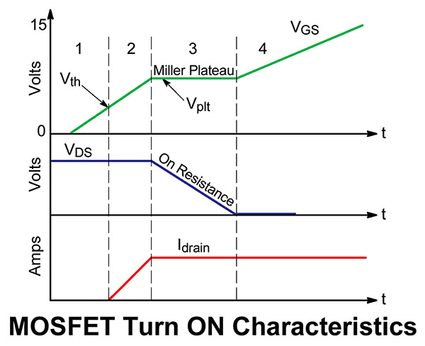
The MOSFET switching time is divided into four sections as shown in Figure 2.
- During this period, the gate voltage (VGS) is charging the input capacitor — which is dominated by the gate-to-drain capacitance (Vgd).
- At Vth, drain current begins to flow. During this time, the drain voltage (VDS) is typically constant at the source voltage (VCC).
- This is the stage where the Miller plateau (Vplt) is reached, at which time the drain voltage — ON resistance — begins to linearly decrease until the end of the third period. This occurs when VDS reaches 10% of its OFF value. It’s during this period that the MOSFET dissipates most power and heat.
- In region 4, the MOSFET is fully saturated, and the ON resistance is at its minimum. VGS continues to increase to its full driving value — typically 15 V.
By increasing the gate voltage, the Miller capacitor can be forced to charge faster, and that decreases the switching time. The discharge time of the MOSFET is a mirror image of this profile, with the Miller plateau discharge time governed by the resistance of RG — the gate input resistor.
Want more MOSFET stuff? Check out “IGBT Basics.”


Comments