I was asked how to design a counter. Counters are a basic digital logic building block and have a multitude of uses.
Counters advance through a consecutive numerical sequence — either up or down — each time a clock pulse is driven. They are used to divide high frequency clocks to yield lower frequency clocks for state machines and basic event counting. You can design a counter from scratch with truth tables by applying Boolean logic.
In this article, we'll discuss using off-the-shelf counter chips to take advantage of pre-fabricated building blocks.
The common 7400 logic family has numerous four-bit counter chips available. Four bits is a popular size because the counter is small enough to fit in a 16-pin package and can be easily cascaded to form longer widths; two four-bit counters give you a byte counter.
A four-bit binary counter normally advances from 00002 to 11112 or 0 to 15 decimal. This natural power-of-two count sequence is useful in many applications.
Some applications, however, are more suited to a decade counter that advances from 00002 to 10012 or 0 to 9 decimal. Decade counters are often used when counting events that are to be interpreted by people, since people tend to think in decimal.
The term binary coded decimal — or BCD — refers to a binary counter that wraps from 10012 to 00002 rather than continuing with a normal binary count sequence.
74LS190 Decade Counter
A well-known decade counter is the 74LS190. It has been around for a long time, as evidenced by the original date of December 1972 on a datasheet I downloaded from the web. The ‘LS190 is a synchronous counter, meaning that it outputs transition only on a low-to-high clock edge. This gives the counter very predictable behavior.
Figure 1 shows the ‘LS190 pin assignment.
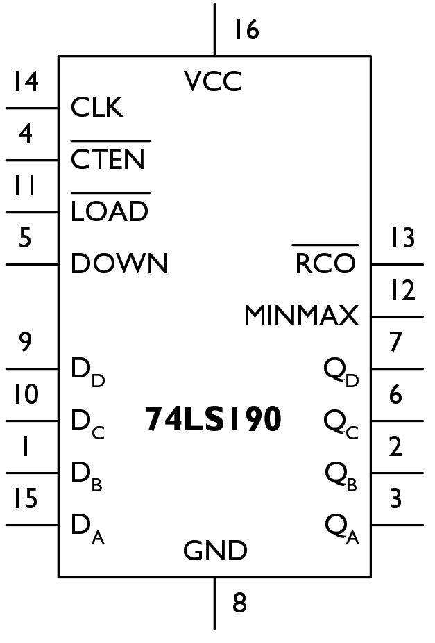
Figure 1. 74LS190 pin assignment.
Aside from two power pins, the chip has four count inputs, four count outputs, a clock, and several control signals. The count inputs, DN, enable pre-loading the counter with a specific value, giving you the option of not always starting the count from zero.
The LOAD signal transfers the DN state inside the chip, which is reflected at the outputs, QN, on the next rising clock edge. We'll use this feature to reset the chip to start counting at zero.
Next, there's a DOWN signal that tells the chip to count down when DOWN = 1 or to count up when DOWN = 0.
Aside from the clock, CLK, there is a count enable signal, CTEN , that qualifies CLK. When CTEN = 0, the chip increments or decrements normally on the clock’s rising edges. When CTEN = 1, the counter does not advance and retains its present value, unless a new value is loaded via the LOAD signal.
CTEN and the two outputs, RCO (ripple carry out) and MAXMIN, facilitate cascading multiple counters to yield practically any size counter.
A Cascaded Counter
So how does this all come together? Figure 2 shows a byte-wide cascaded counter comprised of two 74LS190 chips.
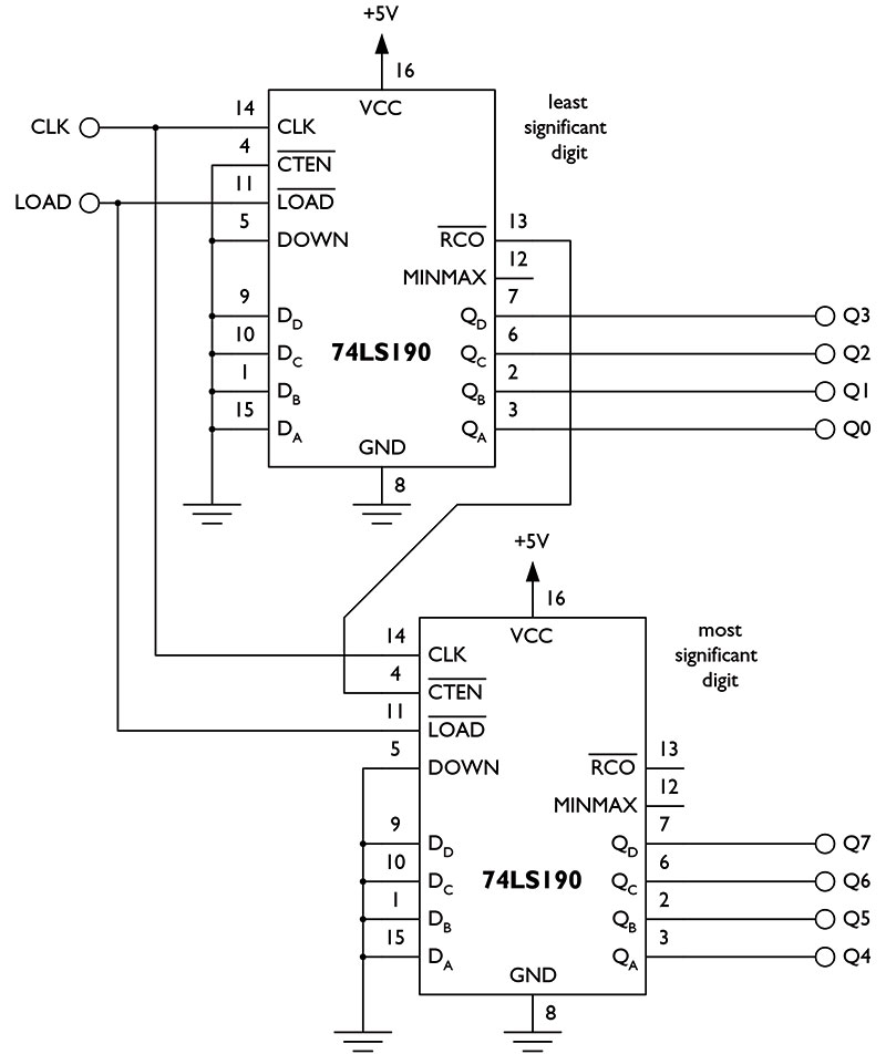
Figure 2. Byte-wide counter.
Note that both chips have common CLK and LOAD signals. This means that both chips can advance together on the same rising clock edge. It also means that they can be reloaded together.
The example has DN tied low so that the counter is reset to 0 when LOAD = 0 and CLK is driven low-to-high. The DOWN signal is set low on both chips to indicate an advancing count sequence from 0 to 9 for each chip.
Finally, the counters are cascaded to form one single counter by driving one counter’s CTEN signal with the other’s RCO signal. The least significant digit’s RCO pulses low each time the count value is 9. This enables the most significant digit’s counter for one clock cycle so that it advances on the next CLK edge.
After this next edge, the least significant digit wraps around to become 0, which restores RCO to its high state and deactivates the most significant digit counter until it is again time to advance.
Control Inputs
At this point, we have the core of a counter circuit but there are two dangling inputs: CLK and LOAD. These can be manual pushbuttons so that you can control when the counter is reloaded with 0 and when it advances. LOAD can be directly tied to a pushbutton.
CLK, however, is not as simple because it regulates the entire circuit’s behavior. CLK must be a clean signal with uniform high-low transitions so that the counter behaves correctly.
If we directly connect a pushbutton to CLK, the counter is likely to behave erratically.
The reason for this is that a mechanical button generates electrical noise as its internal surfaces make and break contact. This noise may be imperceptible to a person, but a synchronous logic circuit will react wildly. A debounce circuit (such as the one shown in Figure 3) can fix this problem.
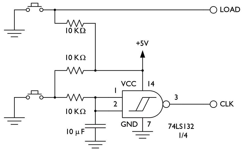
Figure 3. Clock debounce circuit.
As its name implies, a debounce circuit removes the bounce — or noise — from an input and generates a clean output. There are numerous techniques to debounce a pushbutton. The one shown here uses an RC filter along with a Schmitt trigger inverter (made from a NAND gate) to filter out the noisy pushbutton clock signal. The RC time constant is 100 milliseconds when discharging from 5V to 0V and 200 milliseconds when charging back to 5V.
You can adjust the time constant higher or lower to suit your specific needs.
After connecting this portion of the circuit, the counter cleanly increments each time you press the CLK button and reloads when you hold down LOAD and press the CLK button.
Seeing is Believing
The counter is now functional, but doesn't give you very much indication that it may be working as it currently stands.
We need to connect a visual indicator to see what count values are being generated. The simplest thing to do is connect an LED to each of the eight outputs and watch the BCD pattern change with each CLK press.
It's more interesting, however, to read a recognizable 0-99 count sequence. For this, we turn to the 74LS47 BCD-to-seven-segment decoder/driver.
You may observe seven-segment displays all around you: microwave ovens, digital watches, stereos, and VCRs. Each display contains seven independent light elements — often LEDs — that can form a recognizable decimal digit. The 74LS47 converts the BCD output of the 74LS190 into a human-readable, seven-segment format.
Figure 4 shows how one 74LS47 chip connects to the least significant digit of the counter that we have already created.
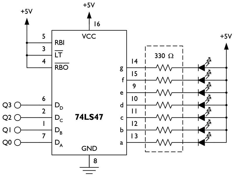
Figure 4. Seven-segment display circuit.
(A second, identical 74LS47 and seven-segment display connect to the most significant digit.)
It's a simple hookup with just three control signals to tie high. The 74LS47 has active-low outputs that are designed for common-anode LED displays.
A common anode display has all of the LED anodes connected to a single pin. The individual cathodes connect to the decoder chip through current-limiting resistors. The resistors prevent too much current from flowing through the LED into the 74LS47 and damaging either. Each segment of the seven-segment display is identified as “a” through “g.”
Counters and More Counters
There is virtually no limit to what you can do with counters. They are present — in one form or another — in almost every complex digital logic circuit. You can design custom counters with your own logic or you can employ off-the-shelf counters.
You can read more about counters, counter design, current limiting, and LEDs.
Fortunately, there are many resources and components available that will allow you to experiment and build whatever counters you are interested in. NV